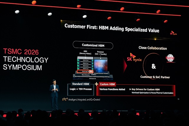
SK Hynix is hiring engineers in San Jose to collaborate on designing 3D stacked DRAM-on-logic chips with US customers. This represents an expansion of the company's custom memory offerings beyond traditional high-bandwidth memory toward on-device AI applications, a move that suggests growing demand for memory solutions tailored to AI workloads.
Summaries like this, in your inbox every morning.
Sign up free →What happened
SK Hynix is recruiting engineers in San Jose to co-design 3D stacked DRAM-on-logic with US customers, according to CDO Ahn Hyun's remarks at TSMC Technology Symposium 2026.
Why it matters
The move extends SK Hynix's custom memory strategy beyond high-bandwidth memory toward on-device AI applications, positioning the company to serve customers developing AI-capable devices that require tightly integrated memory and logic chips.
What to watch
The San Jose recruitment signals SK Hynix's intent to build local engineering capacity for direct co-design partnerships with US technology customers.
SK Hynix is expanding its engineering footprint in the United States by recruiting engineers in San Jose to support a new initiative in 3D stacked DRAM-on-logic co-design. The effort aims to work directly with US customers to develop custom memory solutions that integrate DRAM and logic on a single chip, a technical approach tailored to on-device AI applications. SK Hynix Chief Data Officer Ahn Hyun disclosed this strategy at TSMC Technology Symposium 2026, framing it as an extension of the company's existing custom memory work. Historically, SK Hynix has been known for high-bandwidth memory (HBM) products, which are used in data center AI accelerators. This new push toward 3D stacked DRAM-on-logic represents a shift in focus—from serving cloud infrastructure providers to enabling AI processing at the edge, on consumer and enterprise devices. By establishing local engineering capacity in San Jose, a hub of US semiconductor design and manufacturing activity, SK Hynix is positioning itself to work more closely with customers during the design phase, rather than supplying off-the-shelf memory products. This co-design model allows SK Hynix to tailor memory architectures to the specific needs of devices that must perform AI inference with tight constraints on power and latency.
SK Hynix's recruitment of engineers in San Jose reflects a strategic pivot in how the memory supplier engages with its US customer base. Rather than selling standardized memory products, the company is moving toward co-design partnerships that integrate memory and logic on a single chip—a technical approach suited to the constraints of on-device AI, where latency and power efficiency matter as much as raw performance. CDO Ahn Hyun's public discussion of memory-logic integration at TSMC Technology Symposium 2026 signals that this is not a quiet internal initiative but a competitive positioning statement, likely in response to demand from US semiconductor and device makers building AI-capable products. The shift from high-bandwidth memory (which serves data centers) to 3D stacked DRAM-on-logic (which serves edge devices) suggests SK Hynix sees opportunity in the coming wave of AI inference at the device level rather than solely in cloud infrastructure.
AI-summarized, only the topics you pick — one digest a day via Email, Slack, or Discord.
Free · takes 30 seconds · unsubscribe anytime
No discussion yet for this article
Get curated AI news from 200+ sources delivered daily to your inbox. Free to use.
Get Started FreeFree · takes 30 seconds · unsubscribe anytime