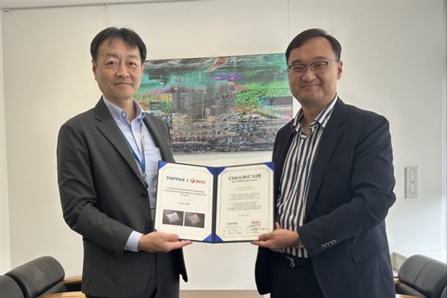
Substrate technology—the physical foundation that connects AI chips to their power and data systems—is emerging as a supply-chain bottleneck as AI packages become larger and more complex. Organic substrates, currently standard, may not deliver the high-density interconnects and low power loss that next-generation AI systems require, pushing the industry to explore glass substrates. Companies like JNTC and TOPPAN are positioning themselves as critical suppliers in this shift.
Summaries like this, in your inbox every morning.
Sign up free →What happened
As AI accelerators and high-bandwidth memory (HBM) packages grow larger and more complex, substrate technology is becoming a new constraint in advanced packaging. Organic substrates remain widely used, but rising demand for high-density interconnects and lower power loss is shifting attention to glass substrates as a potential solution.
Why it matters
Substrate capacity directly limits how many advanced AI chips can be manufactured and deployed. A shift to glass substrates signals that the industry recognizes organic substrates may not scale to meet future density and performance requirements—meaning substrate makers like JNTC and TOPPAN could become critical bottlenecks or enablers in the AI infrastructure supply chain.
What to watch
Whether glass substrate adoption gains traction among major chipmakers and packaging partners, and whether JNTC and TOPPAN can scale production fast enough to meet projected demand as AI systems continue to grow in size and complexity.
Substrate technology—the printed circuit board-like foundation that physically connects AI chips to power and data systems—has traditionally been an afterthought in the chip supply chain. But as AI accelerators and high-bandwidth memory (HBM) packages have grown substantially larger and more complex, substrate performance has emerged as a genuine bottleneck. Organic substrates, which have dominated the market for decades due to their cost and mature manufacturing processes, deliver adequate performance for many applications. However, they face mounting pressure from the demands of cutting-edge AI systems: interconnects must be packed at ever-higher densities to reduce latency and power loss, and thermal dissipation requirements keep climbing as packages consume more power. These requirements have pushed organic substrates toward their physical limits. Glass substrates offer a potential path forward. Glass can support higher interconnect density, dissipate heat more effectively, and maintain signal integrity over longer distances within a package—all critical for AI systems where every millisecond of latency and every watt of power loss affects throughput and cost. Companies like JNTC and TOPPAN, major players in substrate manufacturing, are actively developing glass substrate capabilities, signaling that the industry sees this as a serious and near-term requirement rather than a distant research direction. The transition, however, is not automatic. Glass substrates require new manufacturing processes, longer qualification cycles, and upfront capital investment. But as AI accelerators continue to scale, the economics are shifting in favor of glass: a single advanced AI package might generate enough volume and margin to justify the investment. This substrate shift also reflects a broader reality: the AI hardware supply chain is no longer constrained by chip design or fab capacity alone. It is now constrained by packaging, thermal management, and the foundational technologies that integrate everything together. Substrate makers who can scale glass production reliably could become as critical to AI infrastructure as silicon fabs themselves.
The growth of AI accelerators and high-bandwidth memory packages has exposed a cascading constraint in the hardware supply chain: packaging and substrate technology. For years, organic substrates have been the standard foundation for connecting chips to power and data systems. However, as AI models grow in size and complexity—requiring larger packages with higher transistor counts and denser interconnections—substrate performance has become a limiting factor. The industry cannot simply shrink or optimize its way out of this problem; the physics of organic materials impose ceilings on interconnect density and thermal efficiency that glass substrates may overcome. JNTC and TOPPAN's push into glass substrates reflects a pragmatic recognition that the next wave of AI infrastructure depends on material innovation at the packaging level, not just at the chip level. This shift, if realized, would elevate substrate makers from commodity suppliers to strategic partners in the AI supply chain.
AI-summarized, only the topics you pick — one digest a day via Email, Slack, or Discord.
Free · takes 30 seconds · unsubscribe anytime
No discussion yet for this article
Get curated AI news from 200+ sources delivered daily to your inbox. Free to use.
Get Started FreeFree · takes 30 seconds · unsubscribe anytime
1 minute a day. The AI essentials.
200+ sources · Email / LINE / Slack