
Applied Materials introduced a suite of semiconductor manufacturing systems in July 2026 to accelerate AI chip production, particularly for high-bandwidth memory (HBM) and advanced 3D packaging, and now expects advanced packaging revenues to grow more than 70% in 2026.
The company's systems—including an enhanced DRAM epitaxy system that reduces fab footprint by 20% and new CMP, copper deposition, PECVD, and metrology tools—position it to capture more than 80% of year-over-year wafer fab equipment spending growth in 2026, as data center memory demand remains supply-constrained.
What happened
In July 2026, Applied Materials introduced a suite of semiconductor manufacturing systems aimed at accelerating AI chip production, including an enhanced epitaxy system for DRAM that reduces fab footprint by 20%, plus three new CMP, copper deposition and PECVD systems for advanced packaging, and two eBeam metrology and defect-analysis systems. The company now expects advanced packaging revenues to grow more than 70% in 2026.
Why it matters
Applied Materials' advanced packaging, along with leading-edge foundry-logic and DRAM, is expected to account for more than 80% of the year-over-year growth in wafer fab equipment spending in 2026. The data center memory space remains among the most supply-constrained markets, and as a leading process equipment supplier in advanced packaging, AMAT is positioned to gain throughout 2026 and 2027 as memory chip production ramps up. This concentration of growth opportunity gives the company pricing power and reduces dependence on any single semiconductor technology cycle.
What to watch
Applied Materials' positioning across DRAM, HBM, advanced packaging and process control during the AI-driven semiconductor buildout through 2027, as well as how the company's broad portfolio compares to competitors like Lam Research and Camtek in capturing share of increasingly materials-intensive semiconductor manufacturing.
Ask the AI about this article →
Applied Materials' July 2026 product launches come amid a period of intense demand for semiconductor manufacturing equipment driven by AI infrastructure buildout. The company's focus on HBM and advanced 3D packaging reflects market priorities: as AI systems require higher performance and power efficiency, chipmakers are turning to these more complex packaging technologies, and the equipment to produce them has become a critical bottleneck. The fact that advanced packaging is forecast to represent more than 80% of wafer fab equipment spending growth in 2026 underscores how central these technologies have become to the industry's near-term trajectory.
The data center memory market's supply constraints create a favorable backdrop for Applied Materials. Unlike cyclical semiconductor segments that can swing between feast and famine, memory—especially the high-bandwidth variety used in AI systems—is facing sustained undersupply. This structural shortage gives AMAT visibility into demand through 2027 and enables the company to command stronger pricing. The breadth of its portfolio (DRAM, advanced packaging, process control) also insulates it from overexposure to any single process node or customer technology choice, a meaningful advantage over narrower competitors.
For example, today's edition would include:
AI-summarized, only the topics you pick — one digest a day via Email, Slack, or Discord.
Free · takes 30 seconds · unsubscribe anytimeWhat is AIToday? →
Ask AI anything about this article. Q&As are published on this page for other readers too.
Israeli startup DataAgent Ltd
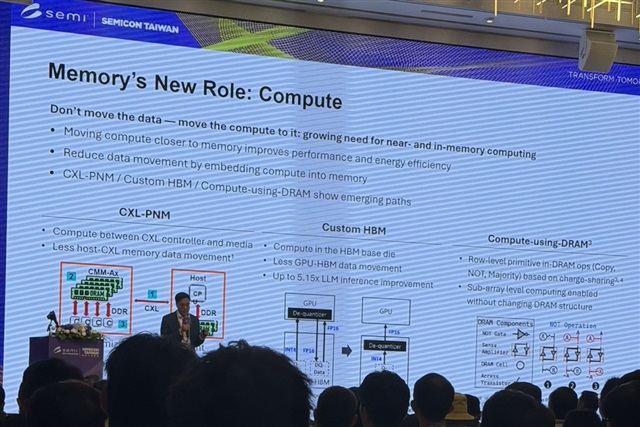
SK Hynix presented a custom HBM concept at SEMICON Taiwan 2026, where compute functions are placed in the base…
Taoyuan is positioning itself as a northern hub for AI data centers (AIDC), citing the Tatan area and an LNG c…
The U.S. Department of Defense announced on August 31 that it has deployed ChatGPT Mil, a customized version o…

Nvidia reported earnings that were both remarkable and boring, reflecting its focus on avoiding a consolidated…

Anthropic has agreed to a $35bn cloud-computing contract with Lambda, a Nvidia-backed cloud provider