AI chips are growing larger, forcing semiconductor packaging to move from 300 mm wafers to square panels.
Glass core is one of several new technologies being developed to support this shift.
Yield in mass production will be critical to success.
What happened
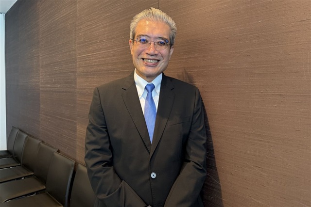
As AI chips grow in size, advanced packaging is moving away from 300 mm wafers toward square panels, with glass core among new technologies being developed in parallel, according to Manz Asia.
Why it matters
The shift reflects a fundamental change in how the semiconductor industry packages increasingly large AI processors. Larger chips require different form factors, and achieving high yield in glass core mass production is essential for viability at scale.
What to watch
Glass core technology is being developed alongside related approaches (FOPLP, CoPoS), signaling multiple competing pathways for next-generation packaging. Yield performance will determine which technologies dominate.
Ask the AI about this article →
The semiconductor industry is undergoing a structural shift driven by the physical demands of modern AI processors. Traditional 300 mm wafer-based packaging, which has dominated for decades, is increasingly ill-suited to chips that exceed the practical bounds of that form factor. Square panels offer a more efficient geometry for larger die, but the industry cannot rely on a single technology to bridge this transition. The parallel development of glass core, FOPLP, and CoPoS suggests manufacturers are hedging their bets while the market sorts out which approach will deliver both performance and manufacturability. For glass core specifically, Manz Asia's emphasis on yield underscores a hard economic reality: a novel packaging technology, no matter how promising, is worthless at scale if it cannot be produced reliably and cost-effectively. Yield—the percentage of functional units from a production run—is the metric that separates viable manufacturing from laboratory success.
AI-summarized, only the topics you pick — one digest a day via Email, Slack, or Discord.
Free · takes 30 seconds · unsubscribe anytime
Ask AI anything about this article. Q&As are published on this page for other readers too.
Samsung Electronics' board approved a 2026 shareholder return plan worth KRW90 trillion to KRW110 trillion (ap…
China Huadian, a state-owned power company, has developed a coordinated model that aligns power generation wit…

Synchrony Financial announced an enterprise collaboration with OpenAI to support AI-native shopping and checko…
Arm Holdings has gained 112.1% year to date and 76.4% over the trailing year, driven by investor enthusiasm ar…

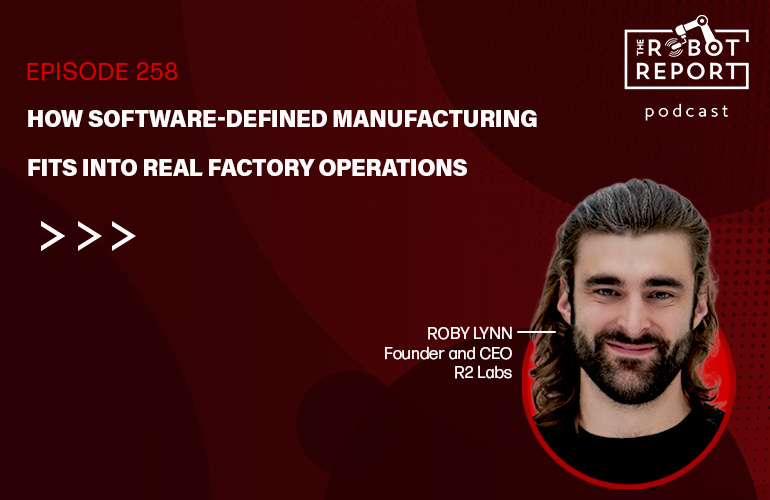
R2 Labs, a Peachtree Corners, Georgia–based smart manufacturing provider, has developed the RAC (R2 Autonomy C…
Nvidia announced a partnership with Cloverleaf Infrastructure on Friday, investing what the Wall Street Journa…