What happened
K&S (Kulicke and Soffa) has expanded its TCB (thermal compression bonding) advanced packaging roadmap, targeting growth in CPO (co-packaged optics) and CoPoS (chip-on-package-on-substrate) applications.
Why it matters
This move positions K&S to address emerging advanced packaging demands, where TCB is a key technology for integrating chiplets and optical components in high-performance computing and AI systems.
What to watch
The roadmap’s success hinges on whether CPO and CoPoS adoption moves beyond early designs into high-volume data center and AI accelerator production, where TCB demand would materialize. Watch for any announced production timelines or design wins from leading AI chipmakers.
Summaries like this, in your inbox every morning.
K&S's expanded TCB roadmap responds to growing complexity in advanced packaging. Traditional packaging methods face limits as chip designs incorporate more heterogeneous components. TCB offers finer pitch connections needed for integrating chiplets and photonics. CPO and CoPoS represent next-generation approaches. CPO aims to bring optics closer to compute to improve bandwidth and power efficiency. CoPoS addresses the challenge of stacking multiple dies with high interconnect density. K&S's focus on these areas suggests the company expects demand to rise alongside AI infrastructure buildouts. Success depends on industry adoption of these architectures, which could shape future packaging equipment demand.
Pick your industry and the AI tools you use, and get news related to your work every day.
Free · 30 seconds with Google · unsubscribe anytimeWhat is AIToday? →
Ask AI anything about this article. The AI reads this article, earlier AIToday articles, and Wikipedia, and cites its sources. Q&As are published on this page for other readers too.
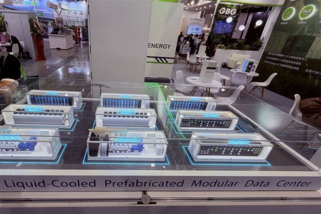
Taiwan-based iBase Solution is expanding from industrial computers (IPCs) and energy storage into liquid-coole…
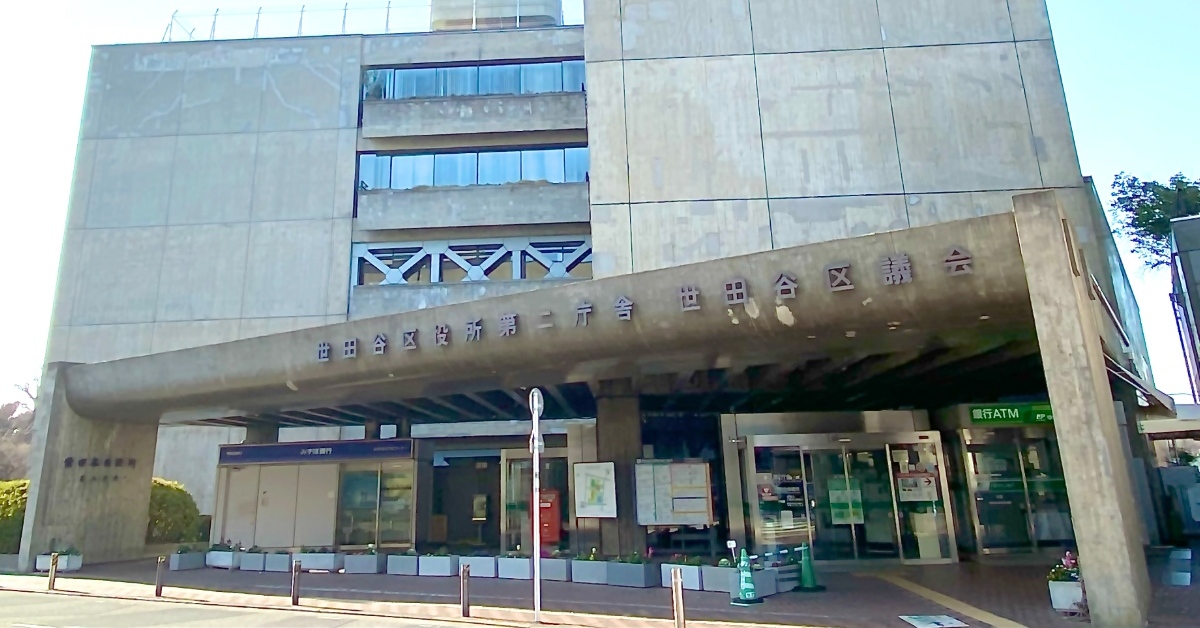
Setagaya Ward tested Genspark, an AI agent tool, and cut roughly 2,900 hours of work, according to Sho Miyama…
Anthropic said it will place 5% of its stock in the Anthropic Public Benefit Fund, pending shareholder approva…
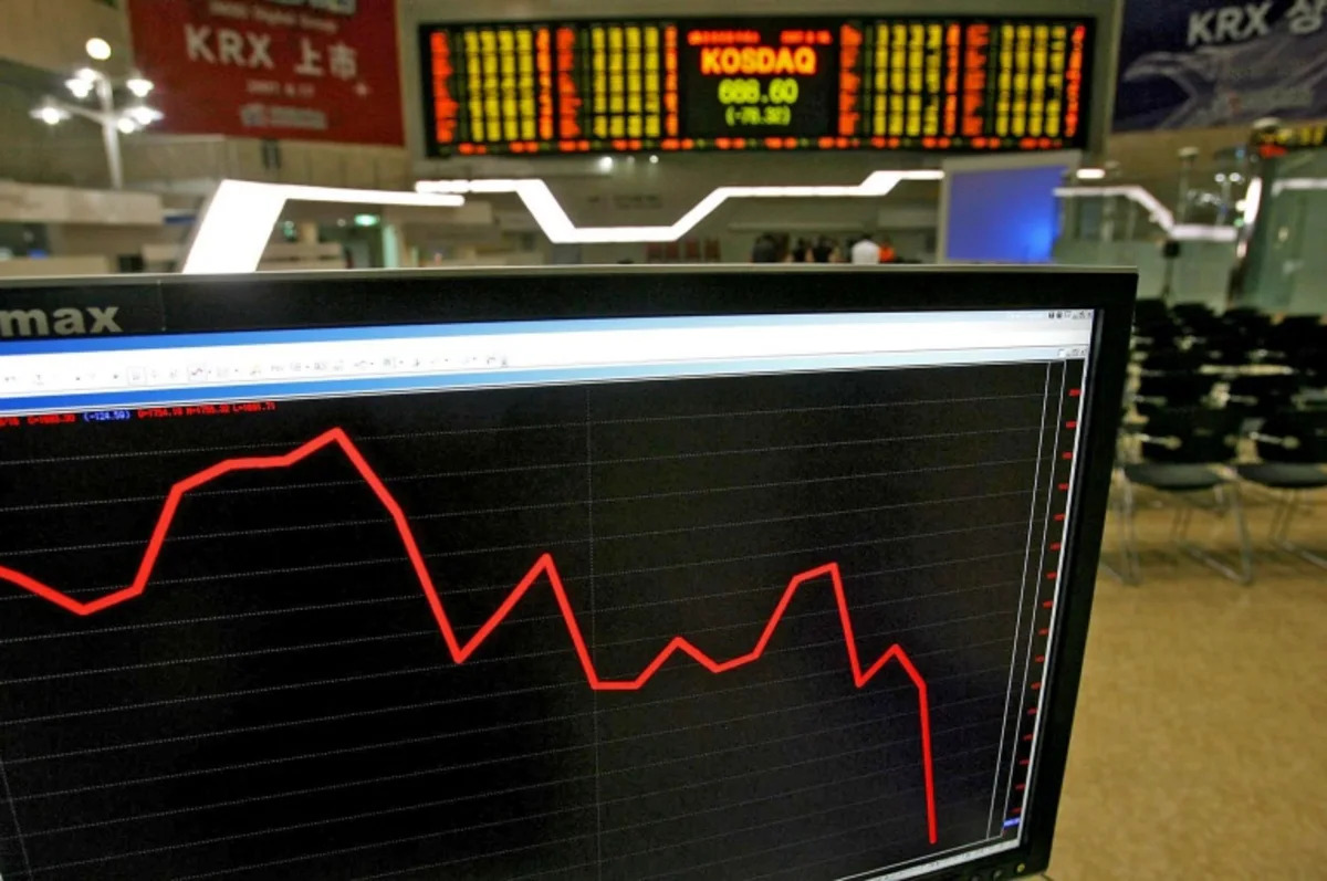
Asian stocks mostly fell Monday after Wall Street's tech-led selloff, with the Nasdaq more than two percent do…
Mercedes-Benz and NVIDIA are expanding their partnership to jointly develop next-generation driver-assistance…
DeepSeek released Search and Fetch APIs on October 17, 2026, with each endpoint priced at $0.75 per 1,000 call…