What happened
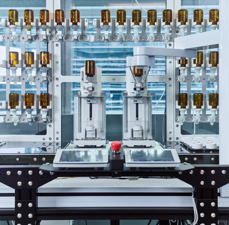
Self-driving laboratory systems—which combine AI agents, simulations, and robotic hardware in a closed loop—are now producing hundreds of novel semiconductor material compositions in weeks rather than years, with results fed back automatically for refinement instead of waiting weeks between manual experiments.
Why it matters
Semiconductor linewidths below 2 nanometers hit quantum tunneling and thermal limits that current materials like copper interconnects cannot handle; new materials are critical to the next chip generation, yet traditional discovery methods still take 10 to 20 years from lab to qualified product—a bottleneck that automation could eliminate.
What to watch
The nearest opportunities are interconnects (where surface and grain-boundary effects dominate sub-10-nanometer scaling), high-k gate materials (where hafnium, now over 20 years old, has risen tenfold in price due to supply constraints), and packaging materials for 3D-stacked architectures that must simultaneously meet mechanical, thermal, electrical, and adhesion targets.
Summaries like this, in your inbox every morning.
Semiconductor manufacturing has long been constrained by the speed of materials discovery, a process that has barely changed for decades. While the industry has automated production-level yield, defect, and process optimization, the discovery stage that determines what materials enter the fabrication plant has been largely untouched. The physics barriers are now acute: linewidths below 2 nanometers trigger quantum tunneling limits and thermal budgets that existing materials cannot support, yet the traditional path from lab hypothesis to qualified product material still spans 10 to 20 years. This sequential, one-experiment-at-a-time approach is poorly suited to the multi-dimensional, multi-property optimization problems modern interconnects, dielectrics, and packaging materials must solve simultaneously.
The emergence of self-driving laboratory systems—which integrate AI agents, atomic-level simulations, robotic hardware, and real-time feedback loops—addresses this bottleneck by running hundreds of candidate compositions and process conditions in parallel and automatically. These systems have already demonstrated the ability to produce novel material compositions in weeks rather than years, with results sent out for independent third-party verification. The critical distinction is that this approach does not skip physical validation; robotic systems synthesize and characterize candidates in real labs, generating the trustworthy data needed to build fab processes. This enables what the industry calls "concurrent engineering"—designing material and product together—rather than the current practice of constraining product design to whatever materials are already qualified. The strategic stakes are high: countries and companies that compress materials discovery will move faster on next-generation chips, reduce supply-chain exposure, and gain a competitive advantage over those still running the decades-long sequential cycle.
Pick your industry and the AI tools you use, and get news related to your work every day.
Free · 30 seconds with Google · unsubscribe anytimeWhat is AIToday? →
Ask AI anything about this article. The AI reads this article, earlier AIToday articles, and Wikipedia, and cites its sources. Q&As are published on this page for other readers too.
Chunghwa Telecom president Rong-shy Lin said the shift from conversational AI to autonomous AI agents is resha…

Apple and Meta said they would jointly release a new open-weight AI model designed to run on high-end Macs, ai…

A writer and entrepreneur opened his daily to-do list and found 156 items, and concluded that an AI assistant…

A Zenn contributor sorted AI use into three modes — AI as an assistant, AI running alongside people, and AI th…

A non-engineer operator says one person ships four smartphone apps on Google Play, three on the App Store, wit…
The walkthrough points the CLI at a local mock via the ANTHROPIC_BASE_URL environment variable