What happened
As AI systems demand greater processing power and energy efficiency, advanced materials — polymers, elastomers, specialty fluids, and other compounds — are becoming the critical constraint on semiconductor fabrication and data center performance. Manufacturers now face extreme challenges: semiconductor fabrication requires thousands of tightly controlled steps with almost no room for error, while data centers shift to higher-voltage architectures and greater power density, intensifying pressure on cooling, power management, and electronic components like connectors and capacitors.
Why it matters
The traditional view of AI progress focuses on algorithms and chip design, but the body supports that materials innovation now directly defines the limits of what is physically possible. Perfluoroelastomers seal semiconductor equipment under extreme temperatures and aggressive plasma; their performance and the sustainability of their manufacturing process now determine whether chipmakers can qualify and deploy next-generation tools. For businesses relying on semiconductor supply chains or operating large AI infrastructure, material constraints may become the binding constraint on speed and scale.
What to watch
Syensqo and other materials companies are using AI tools — including the Microsoft Discovery platform — to accelerate the discovery cycle for candidate materials like next-generation heat transfer fluids for semiconductor and data center cooling. The body indicates that the journey from laboratory discovery to a qualified material will always require scientific expertise and rigorous testing, suggesting that materials innovation timelines remain measured; however, AI is reducing the number of physical experiments required and helping researchers identify the most promising candidates earlier.
Summaries like this, in your inbox every morning.
The article reframes a common misconception about AI's physical foundations. Industry discourse typically emphasizes chip design, algorithms, and investment in fabrication plants and hyperscale data centers — but the body argues that beneath each of these advances lies a layer of advanced materials that now defines the actual limits of performance. This shift in emphasis reflects a real constraint: as each new generation of semiconductors and data center infrastructure demands more processing power, greater energy efficiency, and higher reliability, the materials that support them face increasingly extreme operating conditions — higher temperatures, more aggressive plasma exposure, higher voltages, and greater power density.
The article uses two concrete examples to ground this claim. In semiconductor fabrication, perfluoroelastomers seal equipment under extreme conditions, and manufacturers now expect these materials to be not only higher-performing but also produced sustainably — reflecting a redefinition of what "performance" means. In data center infrastructure, the shift to higher-voltage power architectures is creating materials challenges that parallel those of the electric vehicle industry, suggesting that knowledge transfer across sectors may accelerate solutions. The body indicates that materials companies are responding by using AI-powered discovery tools to reduce physical testing cycles and identify promising candidates faster, though it emphasizes that traditional qualification and rigorous testing remain the gating step — materials innovation will not become instantaneous, even with AI acceleration.
For example, today's edition would include:
AI-summarized, only the topics you pick — one digest a day via Email, LINE, or Slack.
Free · 30 seconds with Google · unsubscribe anytimeWhat is AIToday? →
Ask AI anything about this article. Q&As are published on this page for other readers too.
In a 46-minute interview on CBS, Nvidia CEO Jensen Huang pushed back against apocalyptic warnings about AI and…
China's 15th Five Year Plan (2026-2030) makes embodied AI a top priority, with subsidies and humanoid training…

Apollo's Torsten Sløk told clients the AI spending race depends on hyperscaler operating cash flow more than t…

LG Energy's battery energy storage system (BESS) has qualified into Nvidia's AI Factory ecosystem

China's internet regulator is reportedly investigating DeepSeek and Moonshot AI over allegations they routed m…

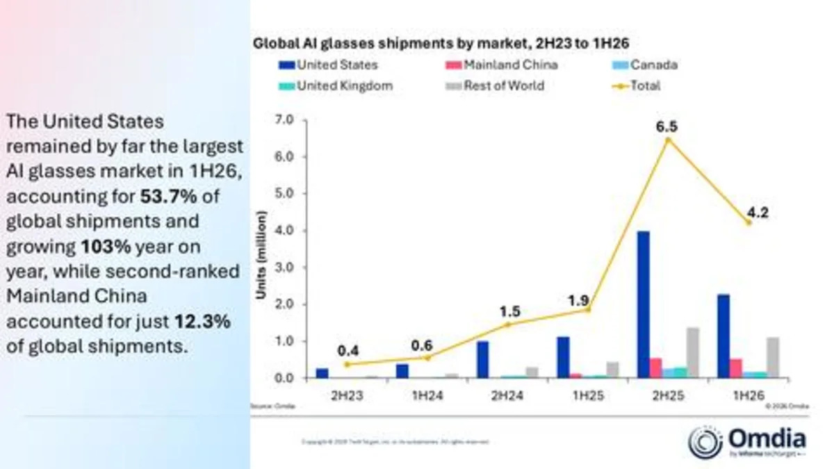
Omdia says global AI glasses shipments reached 4.2 million units in 1H26, up 127% year-on-year, with Meta ship…